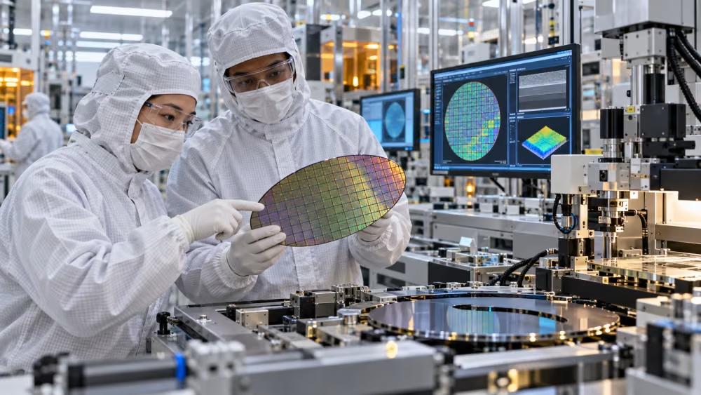
The agreement highlights how U.S. semiconductor growth is expanding beyond chip fabrication into the specialized packaging processes that power advanced computing.
GlobalFoundries and TSMC have signed a five-year, $2 billion manufacturing agreement to establish a U.S.-based supply of silicon interposers for advanced AI chip packaging. GlobalFoundries will add production capacity at its Malta, New York, facility, with volume manufacturing expected to begin ramping in the first half of 2028.
Silicon interposers sit beneath processors and high-bandwidth memory, creating the dense, high-speed connections required by AI and high-performance computing systems. Although less visible than the chips themselves, these components are an essential part of advanced packaging, an area where demand has outpaced available manufacturing capacity.
GlobalFoundries expects the Malta operation to become the first U.S.-based source of silicon interposers supporting advanced packaging technologies. The agreement also provides a framework for further capacity additions as customer demand grows.
The project reflects a broader shift in domestic semiconductor strategy. Building fabrication plants remains important, but a resilient U.S. supply chain also needs packaging, testing, materials, equipment support, and other capabilities required to turn individual chips into complete computing systems.
That expansion has direct workforce implications. Producing advanced packaging components requires employees skilled in precision process control, metrology, equipment maintenance, quality assurance, automation, and cleanroom operations. Employers will also need technicians and engineers who can coordinate production and qualification requirements across multiple companies and manufacturing locations.
No new employment target was announced with the agreement, but the capacity expansion gives educators and workforce partners time to prepare before production ramps. Programs that combine semiconductor fundamentals with hands-on experience in inspection, process equipment, data analysis, and advanced packaging will be well positioned to support this next stage of U.S. electronics manufacturing.
Source note
The primary source is GlobalFoundries’ October 8 announcement(Opens in a new tab/window). Agreement terms and production timing were corroborated by Reuters(Opens in a new tab/window) and Tom’s Hardware(Opens in a new tab/window).